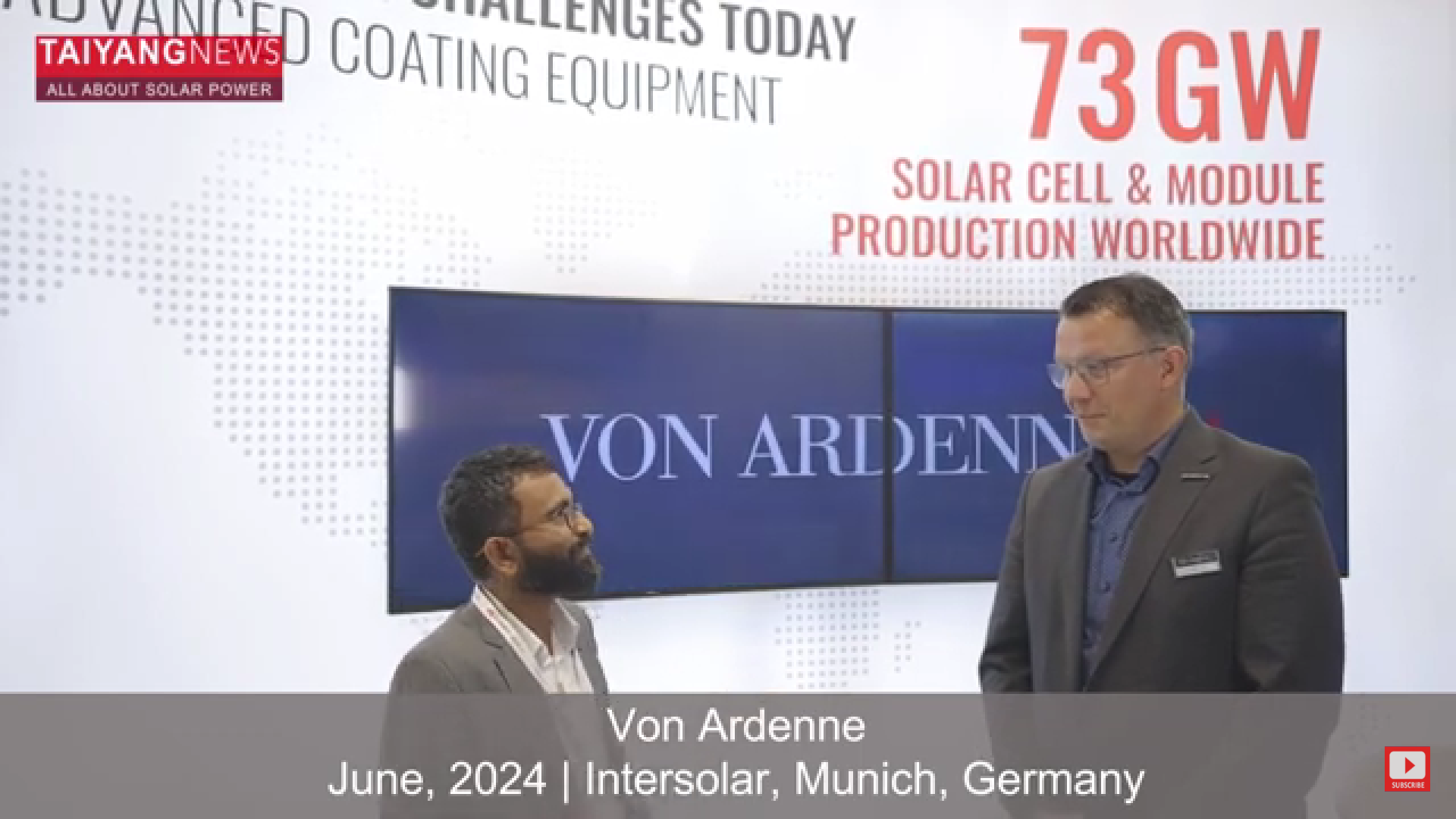
Dresden-based PVD coating technology expert, VON ARDENNE, showcased a wide array of PVD tools based on either magnetron sputtering or evaporation technology at Intersolar Europe 2024. With its global engineering and after-sales service centers, the Germany-headquartered company has supplied 73 GW of PV cell and module production tools worldwide. These PVD coating tools coat either glass or silicon solar cells.
Speaking to TaiyangNews at the event, the company emphasized its portfolio of PVD deposition platforms based on multiple application scenarios – R&D stage, pilot line, market entry, and gigawatt (GW) level mainstream production. The tool maker focused on the latest GW-level GIGA|nova (SCX/DCX) series PVD platform, both with an annual throughput of 1.3 GW.
GIGA|nova DCX
The company also stressed on the GW-scale double-sided horizontal coating platform, known as GIGA|nova DCX. The company says that the inline deposition tool based on magnetron sputtering or linear evaporators for thermal evaporation technology can be suitable for double-side deposition applications in HJT, TOPCon, or tandem perovskite cell mass production. For the HJT cell technology route, this tool can be used for double-sided transparent conductive layer (TCO) deposition. Besides the HJT application, this tool can be useful for the deposition of tunnel oxide (TO) with subsequent n- or p-doped silicon layer for double-sided TOPCon, and ETL, HTL, absorber, TCO, or recombination layers deposition for tandem perovskites (2T) cell structure, added the company. The system, equipped with a wafer handling system, can ensure all requirements for gentle handling of the wafers during loading and unloading despite the enormous speed of the overall system. The system can also be integrated into any line automation concept with interfaces to integrate measuring systems; for example, for breakage detection and quality control. This deposition tool’s throughput depends on the wafer dimensions and the required deposition time, says the company. It says further that a cell tray that can be placed with 180 G/M12 full-size wafers, or 360 half-cut wafers, can be adapted to any wafer size and shape. It adds that a large number of trays pass through the tool with an integrated tray return system that brings the trays back to the wafer loading and unloading system. This system also serves as a buffer, added the company.
Considering a cycle time of 40 seconds and 360 half-cut M12, the GIGA|nova DCX can handle up to 32,400 wafers per hour, explains VON ARDENNE with an example to substantiate its claim of 1.3 GW annual production capacity. The company launched its new double-sided coating platform at the beginning of 2024.
GIGA|nova SCX
This PVD tool is based on a single-sided horizontal wafer coating system that operates based on either sputter deposition by magnetron sputtering or linear evaporators for thermal evaporation. The company notes that the inline deposition tool can be suitable for single-side deposition applications in TOPCon, IBC, or tandem perovskite cell mass production. Single-sided ultrathin tunnel oxide (TO) or silicon dioxide (SiO2) layer deposition with subsequent n- or p-doped silicon layer deposition for TOPCon or IBC TOPCon cell fabrication can be accomplished by the GIGA|nova SCX platform. On the other hand, metal layers like copper (Cu) for IBC and ETL, HTL, absorber, TCO, or recombination layers deposition for tandem perovskites (2T) cell structure can also be possible with this tool, added the company.
VON ARDENNE emphasized that its single-sided PVD deposition route for TOPCon cell application has multiple benefits compared to its peers – no etchback process is needed due to no wraparound, and no toxic gases like PH3 are required. These benefits are attributed to the lack of yield losses due to the deposition and etchback process. Moreover, the lower process cost in the absence of process consumables like PH3 or SiH4 and associated safety requirements contribute to mass-scale production cost optimization. This commercially available single-sided PVD coating platform has the same wafer handling system as the GIGA|nova DCX. Its tray design is a little bit different compared to the GIGA|nova DCX and is optimized for single-sided coating application requirements, the company points out. Considering a cycle time of 42 seconds, yearly production capacities of 1.2 GW and above are achievable – depending on the cell efficiency, and the working hours per year, emphasized VON ARDENNE.
Other products
Apart from the mass-scale production tool, the company offers an entry-level double-sided coating PVD tool platform – XEA|nova L with up to 700 MW throughput. VON ARDENNE also offers PVD deposition tools for pilot line applications under the HISS inline horizontal coating system with up to 100 MW throughput.